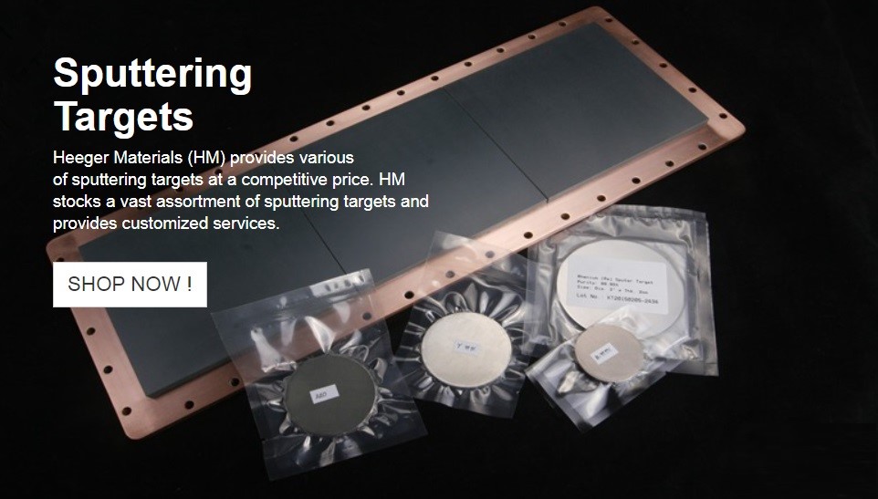
- Working principle of sputtering target
Sputtering is one of the main techniques for preparing thin-film materials. It uses ions produced by the ion source, accelerated aggregation in vacuum, and form a velocity energy ion beam, which bombards the solid surface, and exchanges kinetic energy between the ions and the atoms on the solid surface. The atoms leave the solid surface and deposit on the substrate surface. The bombarded solid is the sputtering targets.
- Second, the components of the sputtering target
The target material is welded by “target blank” and “back plate”.
(1) The target blank is the target material bombarded by the high-speed ion beam, which belongs to the core part of the sputtering target material, involving high-purity metal and crystal grain orientation control. In the sputtering coating process, after the target blank is hit by ions, its surface atoms are scattered by sputtering and deposited on the substrate to form an electronic thin film.
(2) The back plate plays a major role in fixing the sputtering target material, involving the welding process. Due to the low strength of high-purity metal, the sputtering target needs to be installed in a dedicated machine to complete the sputtering process. The interior of the machine is a high-voltage and high-vacuum environment. Therefore, the sputtering target blank of ultra-high-purity metal needs to be joined with the back plate through different welding processes, and the back plate needs to have good electrical and thermal conductivity.
- Third, the process of sputtering target coating
The main processes of coating are physical vapor deposition (PVD) and chemical vapor deposition (CVD).
(1) PVD technology is the current common coating method, and the sputtering process is widely used in semiconductors and display panels. PVD technology is divided into vacuum evaporation method, sputtering method and ion plating method. All the three methods have their own advantages and disadvantages: the vacuum evaporation method has no limitation on the substrate material; the sputtering method has better properties and uniformity than the evaporation film; the ion plating method has strong winding ability and simplifies the cleaning process. The power affects the coating quality. The choice of different methods mainly depends on the product usage and application scenarios.
(2) CVD technology mainly generates thin films through chemical reactions. At high temperature, one or several gas-phase compounds or simple substances containing film elements are introduced into the reaction chamber, and a chemical reaction is carried out on the surface of the substrate to form a film.
